The semiconductor industry places the strictest demands on factory equipment. After all, that’s the only way to ensure cleanliness, precision and safety.
Factory equipment engineering for semiconductor manufacturing – an overview:
- AI applications are causing massive growth in the semiconductor industry
- Semiconductor manufacturing happens at the frontend and the backend
- Factory equipment must be suitable for use in cleanrooms, and also be ESD-safe and EMC-safe
- Equipment must not cause any contamination, vibration, or outgassing
- Particle-free transport, safety, durability, and chemical resistance are also decisive
- Typical factory equipment includes cleanroom work benches, mini-environments, transport trolleys and robot cells
- The item Building Kit System offers ideal solutions for all these requirements
Everyone is talking about artificial intelligence (AI) right now. It’s also key to growth. According to Grand View Research, the global AI market is set to hit a volume of 1.81 trillion dollars. In 2024, it already amounted to 279.2 billion. The semiconductor industry is a direct beneficiary of this development, as it supplies the microchips that are essential for AI applications.
This effect can be seen in the global sales of the semiconductor industry. According to Deloitte, sales exceeded expectations in 2024, reaching 697 billion dollars. The consulting agency sees a realistic chance sales will hit one trillion dollars in 2030.
Semiconductor production needs top-quality cleanroom solutions, and that includes a whole variety of factory equipment. The modular item Building Kit System provides the perfect foundation for safe, reliable factory equipment engineering in semiconductor production.
Cleanroom technology for the semiconductor industry
Whether as supplier or manufacturer, item is your reliable partner for cleanroom solutions in the semiconductor industry.
What steps are involved in semiconductor production?
- Semiconductor production is a wide-ranging process that consists of two main phases: front-end and back-end manufacturing
- Front-end manufacturing involves generating the actual circuits on a ready-made wafer. The wafer production is an upstream process that is generally viewed as separate
- Back-end manufacturing relates to the combining, packaging, and final testing of the chips
Front-end manufacturing is made up of the following steps:
Chemical Vapor Deposition (CVD) / Physical Vapor Deposition (PVD)
Thin layers of materials are applied to the wafer. CVD uses chemical reactions to lay down layers. PVD, on the other hand, uses physical methods.
These layers often provide the basis for the later structural and electrical properties of the microchip.
Oxidation
The wafer is subjected to an oxidation process, during which a thin layer of silicon dioxide is applied to the surface of the wafer. This layer acts as an insulator and provides protection for subsequent process steps.
Ion implantation / photolithography
Ion implantation is a process that precisely introduces dopant atoms into the silicon in order to change its electrical properties. The next step is photolithography.
This process projects specific patterns onto the wafer that will define the structure of the semiconductor’s structural elements. Yellow light in the room ensures that structures are not inadvertently exposed.
(Plasma) Etching
After photolithography, etching is used to remove unwanted material and apply the desired pattern to the wafer.
Depending on requirements, either a dry etching process or a wet etching process is used.
Vertical ovens (with potential return to ion implantation / photolithography)
A vertical oven is where thermal processes are carried out, such as diffusion or further oxidation, in order to modify or improve material properties.
This step may be followed by further photolithography and ion implantation to create additional structures.
Wafer Sensor
Once the structural processing has been completed, each chip on the wafer is tested. This includes testing the electrical properties and identifying defective units.
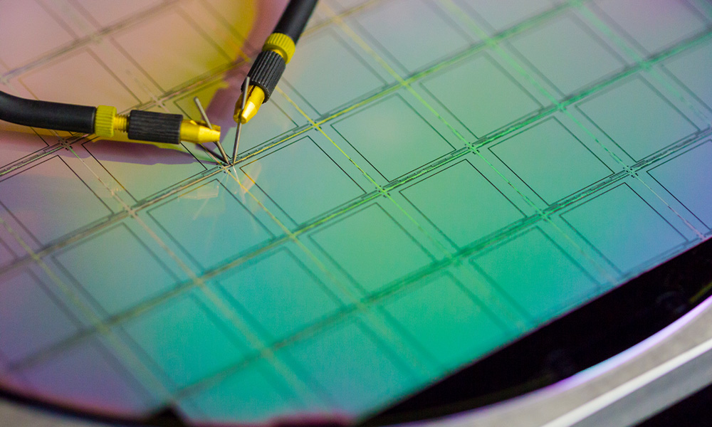
Needles create the contact with the circuits on the surface of the chips during the test process
Once this is complete, the chips move to back-end manufacturing:
Test
This is a detailed inspection of the functional integrity of the chip. Electrical tests ensure that only functional chips are processed any further.
Wafer dicing (die singulation)
The wafer is cut into individual chips (“dicing”). These individual chips are then collected for further processing.
Packaging
Each microchip is packaged in a protective housing. This packaging protects the chip from physical damage and environmental influences.
The packaging also makes it possible to connect the microchip to external circuits.
Device fixing / bonding
This step is when the chips are connected up via connecting wires and contact pads. Processes such as wire bonding and flip chip are used to create electrical connections.
Final Test
Next is the final inspection, during which the packaged chips are tested again to ensure they are fully functional. If chips pass this test, they are ready for use in electronic devices.
What are the challenges in factory equipment engineering for semiconductor production?
Fundamentally, there are still no uniform standards in the semiconductor industry. Standards are defined differently, depending on the company and production stage. However, there are typical challenges and corresponding solutions.
Cleanroom compatibility
Factory equipment for semiconductor manufacturing has to be designed in such a way that it meets the stringent cleanliness requirements of the necessary cleanroom classification. In addition, equipment must be easy to clean and not release any particles that could contaminate production.
Recommendations:
- Avoid open grooves. Line XMS from item provides closed grooves. This simplifies cleaning and creates joins that have very small gap dimensions.
- Specially developed, silicone-free products should be used.
- Wherever possible, horizontal surfaces should be at a slight angle to reduce particle accumulation. This includes the tops of cabinets and machine cabins.
ESD
ESD plays an especially critical role in semiconductor production, where even tiny electrostatic discharges can seriously damage sensitive components.
Recommendations:
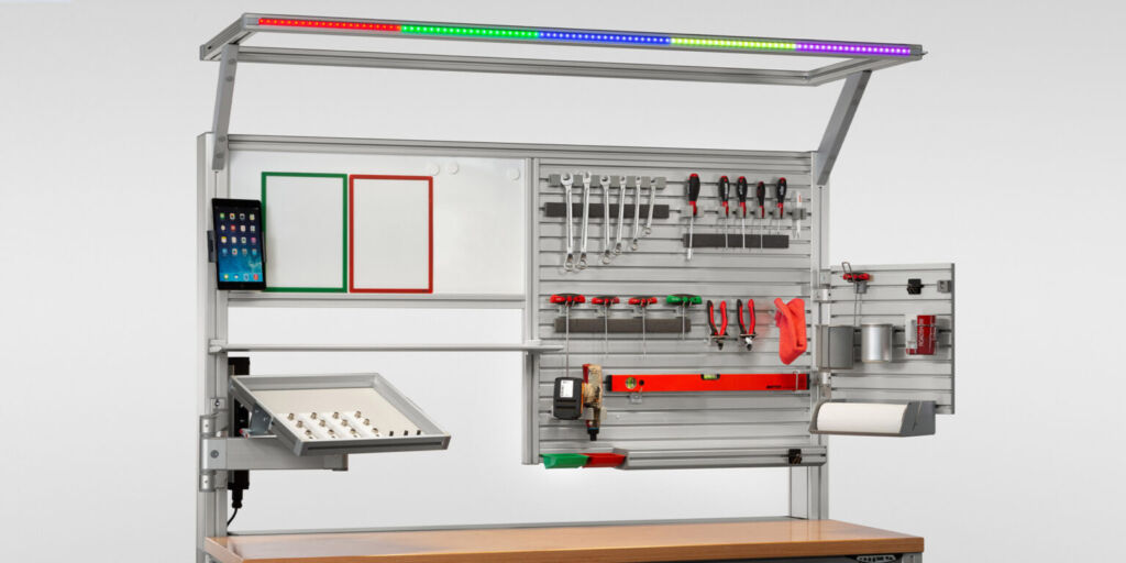
- ESD-safe work benches and appropriate accessories from item ensure all-round protection. Before each work bench is delivered, specialist staff take special measurements. You will receive an ESD record with your delivery as proof of a properly designed solution with the correct discharge resistance.
- Please note: Stainless steel is frequently used in cleanrooms, but this material dissipates abruptly, and is therefore not ESD-safe.
- You can find online training units on ESD in the free item Academy
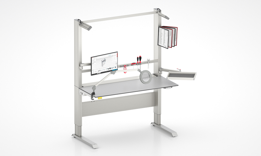
The item Work Bench: cleanroom-compatible, ESD-safe, ergonomic
EMC
Electromagnetic compatibility (EMC) is essential in the semiconductor industry. Housings must therefore be shielded against electromagnetic interference.
Recommendations:
- Use panel elements that provide shielding and (wherever possible) Profile KH. This profile is not cleanroom compatible or resistant to chemicals, but it is perfect for areas where these characteristics are not required, but EMC protection is.
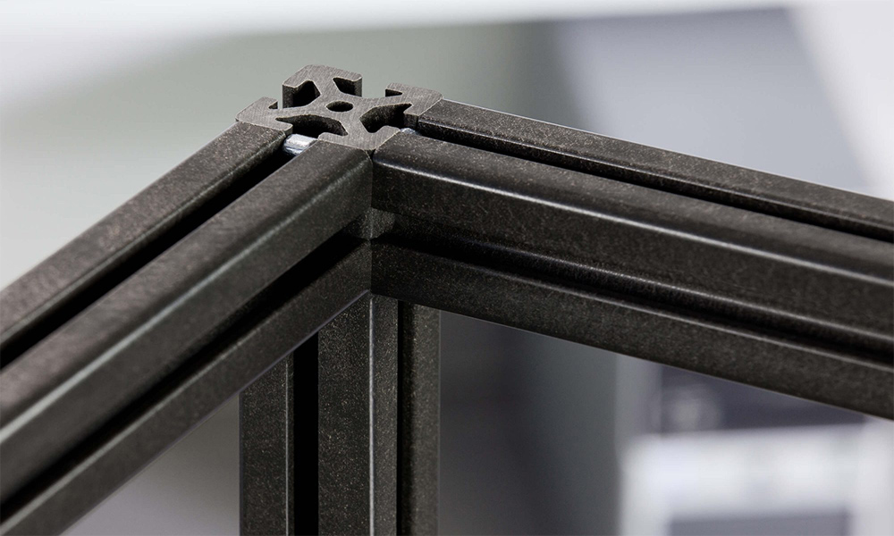
Thanks to its insulating characteristics, Profile KH is perfect for EMC protection.
Contamination checks
No contamination can be permitted to enter the cleanroom throughout the entire semiconductor manufacturing process. The factory equipment must ensure this is the case, for example by using HEPA filters.
Recommendation:
- Our filter fan units (FFU) help you meet this requirement, for example in machine housings and workstations.
Damping vibrations and shocks
Transport solutions for cleanrooms must generate minimal vibrations so as to prevent damage to the wafers and the structures applied to them. This aspect is particularly important in the production of the most delicate structures.
Recommendation:
- Use suitable floor elements and cushioned surface coverings, and incorporate additional weight during design to provide greater stability.
Avoiding outgassing
In semiconductor production, the materials and components must not cause any outgassing. Above all, you should avoid silicone and PVC. This is how you can safeguard cleanliness and safety in sensitive production environments.
Recommendation:
- Many of our cleanroom products meet these requirements. When bought-in parts such as automated elements are incorporated, the solution will need to be specially tested
Particle-free transport
Transport solutions must ensure that as few particles as possible are released, otherwise, the wafers would be contaminated.
Recommendation:
- The choice of panel elements is particularly important. Especially when it comes to ESD protection, conductive polyurethane (PU) and conductive polyamide (PA) are the materials of choice. In addition, Plastic Pro from item is ideal
Safety and documentation
Compliance with safety standards and comprehensive documentation have top priority in semiconductor manufacturing. This is the only way to ensure you meet all regulatory requirements.
Recommendation:
- Ideally, you should design your solutions directly in the item Engineeringtool. In this way, you not only benefit from significant time savings during the design process, you also have detailed documentation for your factory equipment
Only certain materials allowed
Zinc, tin and similar materials are not permitted. These lead to corrosion and microscopically small growths of zinc (“zinc whiskers”). By not using these materials, you ensure a high level of durability.
Recommendation:
- There is not always contact with corrosive materials. In such cases, aluminum can be used, for example. Otherwise, it is advisable to use Profile St from item, which is made from corrosion-resistant steel, and stainless steel surfaces. In any case, resistance to any chemicals used must be tested.
Chemical resistance
The semiconductor industry uses aggressive chemicals. Certain contact surfaces on factory equipment such as racks, tables and shelves must be made of chemical-resistant materials.
Modular aluminum profiles are very popular in the industry due to their lightweight design and, above all, their flexibility. However, aluminum is prone to corrosion caused by aggressive chemicals such as hydrofluoric acid (HF), nitric acid (HNO3), sulphuric acid (H2SO4), hydrochloric acid (HCl) and tetramethylammonium hydroxide (TMAH). Careful analysis must be undertaken as to whether the item aluminum profile technology will come into contact with these chemicals.
Recommendation:
- Plastic Pro can often be used in place of stainless steel. It is important to check chemical resistance beforehand.
What factory equipment is typically used in semiconductor production?
Here are some examples of typical factory equipment used in semiconductor production:
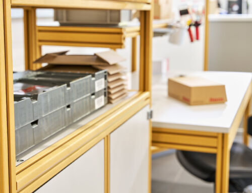
Work benches and storage racks for cleanrooms
These solutions are often made from aluminum, stainless steel, or antistatic materials. This makes it possible to rule out particles and ensure materials can be stored without risk of contamination.
Mini-environments
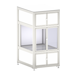
Shielded micro-areas within a larger cleanroom are common in semiconductor manufacturing. Mini-environments or laminar flow boxes isolate especially critical process steps. Cleanliness is maximised in a targeted way and contamination is prevented.
This provides greater control over air quality, temperature and pressure in sensitive areas, while the remaining areas of the cleanroom do not have to be brought up to the highest cleanliness standards.
The advantages of mini-environments:
- Improved contamination control
- Increased flexibility
- Reduced operating costs
Mechanical door locks
Door locks are used in cleanroom airlocks. They ensure that both doors can’t be opened at the same time. Our Security Lock is ideal for this.
(Door) Seals
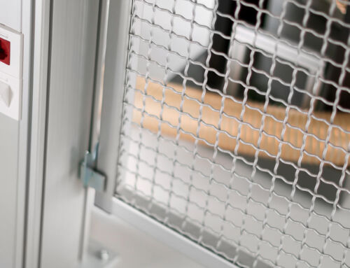
These components are key to ensuring all doors and openings in a cleanroom have an airtight seal. This prevents contamination. The item Access Door system offers flexible options for this.
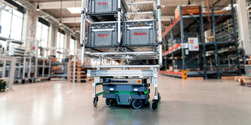
Manual material transport trolley
Use the modular item building kit principle to create special trolleys that transport materials in the cleanroom without releasing particles.
Robot islands
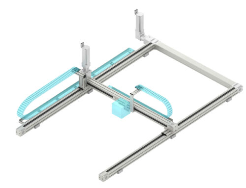
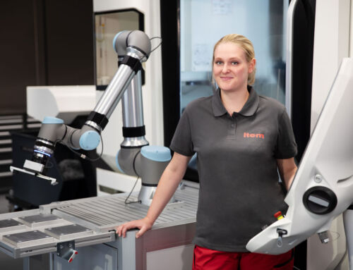
With a mobile robot island made from cleanroom-compatible profiles, you can move your cobot quickly to where it is needed.
There aren’t many cobots that meet the more stringent cleanroom requirements, but the KUKA LBR iiwa is among those that do (up to ISO class 2/3). There are specialist SCARA robots for the highest cleanroom class (ISO 1), but no conventional cobots.
Are you interested in solutions for semiconductor manufacturing? Then we have something that’s right up your alley! Simply subscribe to the item blog today!
