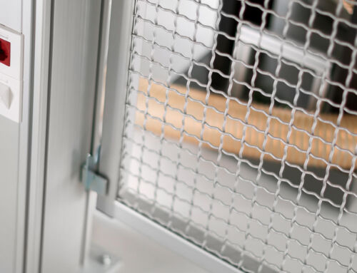
Cleanrooms for chip production – understanding the requirements
Microchips are at the heart of many products, but a semi-conductor shortage is slowing down innovation. The aim of the European Chips Act is now to boost production in Europe. Here, we explain the requirements associated with semi-conductor production.
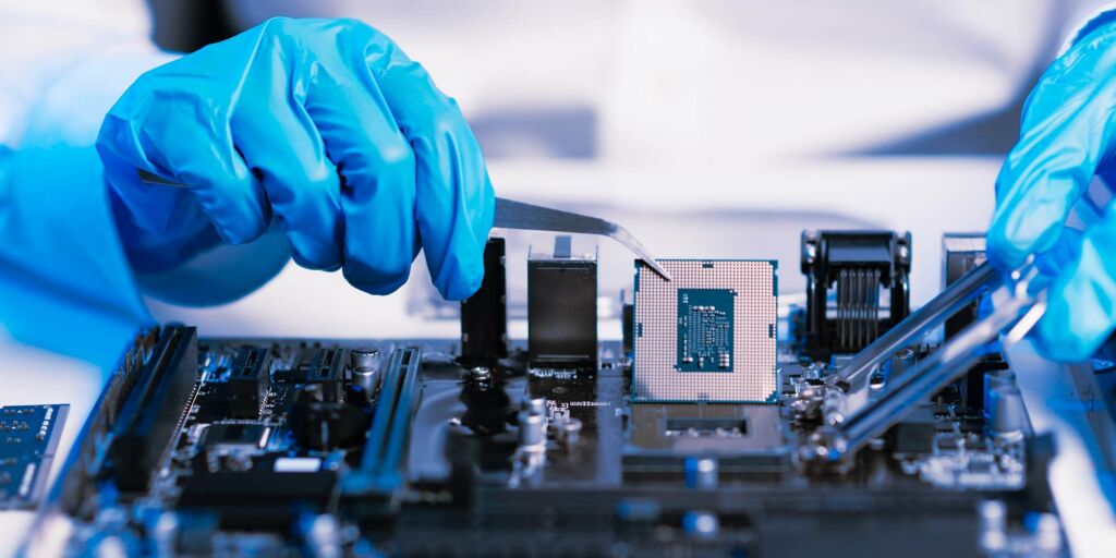
What do cardiac pacemakers, alarm systems, mobile phones and industrial robots have in common? They are all based on microchips. These chips are the backbone of many products, from life-saving medical devices to machines that keep our factories running. Chip production must take place in a clean room.
With its European Chips Act, the European Commission wants to increase production capacities for semi-conductors in Europe. This should make supply chains more stable and reduce dependence on imports. For small and medium-sized enterprises (SMEs), this presents both an opportunity and a challenge. The item Building Kit System offers suitable solutions to help you meet the stringent cleanliness and functional requirements applicable to semi-conductor production.
System solutions for cleanrooms
Use the modular design principle to create dependable cleanroom solutions! Whether you need a work bench with laminar flow box, a cleanroom cabin or a partial enclosure, item will help you implement solutions in exactly the dimensions required.
The European Chips Act and what it means for SMEs
The European Chips Act is an important step for bolstering the competitiveness of the semi-conductor industry in Europe. The regulation, which entered into force on 21 September 2023, is intended to lead to more secure supply chains and greater independence from countries outside Europe. Only 10% of the world’s microchips are currently produced in Europe. One aim of the European Chips Act is to double this figure to 20% by 2030. A total of 43 billion euros is being made available to help achieve this aim, with targeted funding for innovations in the areas of design, manufacturing and packaging. Additional aims of this legislation are to create an investment-friendly environment for new manufacturing plants (fabs), expand production capacity, stabilise the supply chain and create jobs. You can find more details about the Chips Act in the European Commission’s Fact Pages.
One aim of the European Chips Act is to double the proportion of microchips produced in Europe from 10% to 20% by 2030.
At present, Asia and the USA are the dominant players in the global semi-conductor market. Europe therefore needs to remain competitive to protect its industry against production stoppages. Consequently, the European Chips Act is providing SMEs with targeted support to boost their innovative strength and production capacities. SMEs play a key role in this context, because they frequently offer flexible, specialised solutions that are crucial for innovations in the semi-conductor industry.
What is important now – cleanroom technology for silicon wafers and chips
The European Chips Act will set the semi-conductor industry on a growth trajectory. This will provide opportunities for SMEs, but that’s not the only factor to consider – to be successful in this highly dynamic market, the right conditions for production need to be in place, too. Cleanrooms play a key role in this regard, because a clean, low-particle environment is vital in order to ensure high-quality microchips. Even the tiniest amount of contamination can lead to significant production stoppages. Microchips are needed in almost all branches of industry – from the automotive sector to medical technology.
In the semi-conductor industry, there are still very different views on approaches and standards. This could pose a challenge for the European Chips Act.
Major manufacturers and suppliers, such as Zeiss, ASML, Infineon and Intel, already use state-of-the-art cleanroom technology. For SMEs that are starting out in semi-conductor production or want to expand their capacity, investing in suitable cleanroom technology is a must. Kevin Haas, a cleanroom expert at item, foresees a particular challenge when it comes to implementing the European Chips Act. “There are still some very different opinions regarding the requirements in the semi-conductor industry. Companies are only familiar with general cleanroom requirements. However, if the growth forecasts are to be achieved, top-quality cleanroom solutions will be needed,” he explains. The structure size in the semi-conductor industry, i.e. the distance between individual conductor tracks, is becoming smaller and smaller and is in the nanometre range. Therefore, the manufacturing processes need to become increasingly sophisticated, too. Specifications and manufacturing tolerances are also becoming ever narrower.
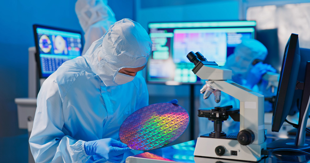
Semi-conductors are produced in cleanrooms. Here, an employee inspects a silicon wafer.
Requirements in the semi-conductor industry
SEMI is an organisation that has produced various guidelines for manufacturing wafers. However, not all companies in the semi-conductor industry use the guidelines in the same way. Below is a list of the key requirements for this sector that you should always bear in mind:
- Rustproof components – to prevent corrosion and contamination
- Minimal outgassing – to prevent contamination by gaseous substances
- High level of cleanliness – no dust deposits thanks to easy-to-clean surfaces
- Flexible reconfiguration – adaptability in line with changing production requirements
- ESD safety – protection against electrostatic discharges
Requirements relating to semi-conductor production are very stringent and often vary, depending on each company’s particular specifications and production steps. There is no single universal standard that comprehensively governs all requirements, nor are there any strict regulations about the materials used in fasteners and plastics. There is, however, one point on which companies in the semi-conductor industry agree – when selecting materials, it is important to ensure that the reject rate can be kept as low as possible. You should avoid using materials that could cause corrosion or contamination in the cleanroom, and opt instead for anodized aluminium, stainless steel or glass. The key concept here is what is called the first pass yield. First pass yield (FPY) refers to the percentage of products that successfully emerge from a production process first time round, without needing to be reworked or repaired. A high FPY is crucial for maximising efficiency and minimising costs.
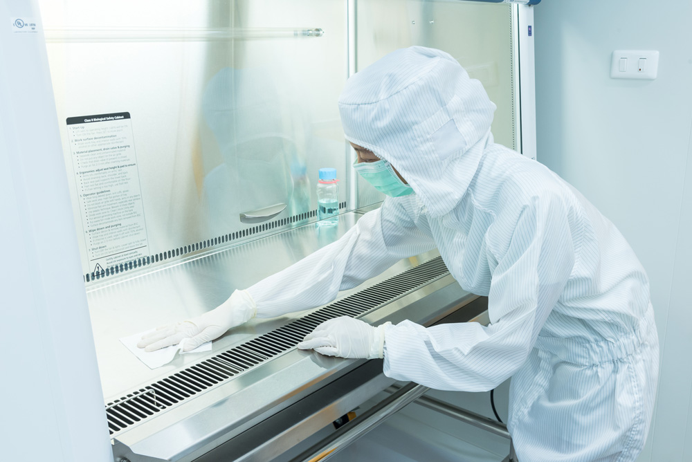
When producing chips in a cleanroom, maximum cleanliness is crucial.
item cleanroom solutions for chip production
In semi-conductor production, it is vital to exclude any chance of products being contaminated with even the smallest particles – the objective is zero-defects production. To achieve this, lots of different elements need to work together reliably. You need certified components that are tailored to your needs – and this is exactly where the item Building Kit System comes in. You can use this system to set up cleanrooms that meet the requirements of cleanroom classes in accordance with DIN EN ISO 14644-1. With item, you can build cleanroom-compatible solutions, such as work benches, cabins and enclosures, and establish maximum precision in chip and wafer production. Thanks to a large selection of profiles and accessories, you can build cleanroom solutions in exactly the size, shape and configuration you need. What’s more, you can design work benches that are cleanroom-compatible, ESD-safe, ergonomic and functional. Here are some examples of components and solutions from the item Building Kit System for your cleanroom:
In semi-conductor production, it is vital to exclude any chance of products being contaminated with even the smallest particles – and this is exactly where the cleanroom-compatible item Building Kit System comes in.
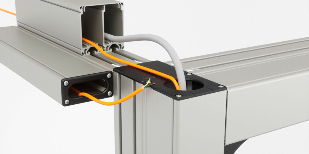
Our cleanroom-compatible aluminium Profiles X and XMS feature a minimal edge radius and unbroken outer surfaces. They are therefore ideal for easy-to-clean machine frames. Their properties include the option of laying cables in the profiles, only as many open grooves as necessary, and a surface that is easy-to-clean and not damaged by cleaning agents. You can use the modular Fixing System for flush surfaces to construct cleanroom-compatible walls and ceilings. The smooth, unbroken surfaces of the aluminium profiles offer two key advantages – they prevent particle deposits from forming and can be cleaned perfectly.
Cleanrooms for semi-conductor production – how we can support you
The semi-conductor industry is one of the driving forces of today’s economy and offers major opportunities for SMEs. By making the correct investments in appropriate cleanroom technology and taking advantage of funding available under the European Chips Act, even smaller companies can remain competitive and make their production efficient.
The item Building Kit System helps you develop bespoke solutions for specific requirements. What’s more, it complies with the stringent precision and safety requirements that are applicable to semi-conductor production.
The item Building Kit System helps you develop bespoke solutions for specific requirements. Our components are simple to install and exceptionally versatile, too. This makes it easier for you to comply with the stringent precision and safety requirements that are applicable to semi-conductor production. What’s more, the high level of delivery reliability at item guarantees that you will be able to get the components and profiles you need quickly – and all in consistently high quality.
